
From the smartphone in your pocket to the world’s fastest supercomputers, the CPU is the engine powering modern technology. Yet today’s processors are far more complex than simple clock speeds and core counts suggest. As performance demands grow, chip design has evolved into a sophisticated balance of efficiency, parallelism, and intelligent resource management. This modern cpu architecture analysis breaks down what truly drives computing power, from multi-core processing and cache hierarchies to instruction sets and emerging design philosophies. By the end, you’ll have a clear understanding of how today’s CPUs work—and where chip innovation is heading next.
Core Concepts: From Single-Core to Multi-Core Dominance
The shift from single-core, high-frequency processors to multi-core designs didn’t happen overnight. In the early 2000s, chipmakers pushed clock speeds past 3GHz, but heat, power leakage, and diminishing performance returns created a wall. Simply put, cranking up GHz became inefficient and expensive. So, instead, engineers added more cores.
A core is an independent processing unit capable of executing instructions. A thread, meanwhile, is a virtual execution path within a core, enabled by technologies like Hyper-Threading. Think of a kitchen: multiple chefs are cores, and each chef’s two hands are threads. More chefs mean more dishes cooked simultaneously; more hands help each chef multitask.
As a result, multi-core CPUs dominate parallel workloads like video rendering or running many apps. However, some legacy software and certain games rely on single-threaded performance, where fewer, faster cores can still shine.
That’s why Instructions Per Clock (IPC) matters more than raw GHz today: IPC measures how much work a core completes each cycle. In modern cpu architecture analysis, higher IPC often outweighs frequency. So, what’s next? Expect questions about core counts, hybrid designs, and AI-accelerated workloads—because the future isn’t just more cores, but smarter ones and efficiency.
The Memory Hierarchy: How Cache Speeds Everything Up
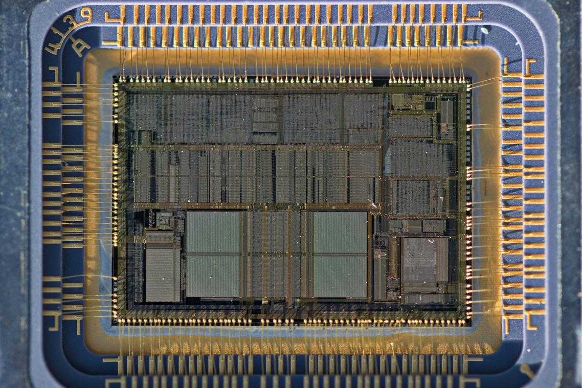
CPUs today can execute billions of cycles per second, while system RAM responds in mere nanoseconds that still feel glacial by comparison. The result is a bottleneck: processors stall, waiting for data. Cache bridges that gap, keeping frequently used instructions close to the cores.
First, L1 cache is the smallest and fastest, sitting per-core like tools strapped to your belt. Next, L2 is larger and slightly slower, still per-core, more like the toolbox beside your workstation. Then L3, shared across cores, acts as the main cabinet in the lab. Beyond that lies RAM, the hardware store across town.
In gaming engines such as Unreal or data-heavy Python workloads, larger caches reduce expensive memory fetches, improving frame times and throughput. That is why modern cpu architecture analysis obsesses over cache latency charts and die layouts. Without cache, would your RTX-powered rig feel fast?
Instruction Set Architectures: The CISC vs. RISC Debate
An Instruction Set Architecture (ISA) is the fundamental language a CPU understands—the set of commands that tells hardware what to do. Think of it as the CPU’s vocabulary. If software is the script, the ISA is the grammar.
CISC (Complex Instruction Set Computer)
CISC, used by x86 processors from Intel and AMD, is built around doing more with a single instruction. One command can handle multiple low-level operations (like loading data and performing arithmetic together). This design helped early developers write compact programs when memory was expensive. Today, CISC dominates desktops and many servers.
Practical example: If you’re building a high-performance workstation for video editing or gaming, you’ll likely encounter x86 chips.
RISC (Reduced Instruction Set Computer)
RISC, used by ARM and Apple Silicon, favors simpler, faster instructions. Each command executes quickly, improving efficiency and lowering power consumption. That’s why smartphones and ultralight laptops rely on ARM.
- Fewer cycles per instruction
- Lower heat output
- Longer battery life
Pro tip: For edge deployments, power efficiency often outweighs raw peak speed—see edge computing vs cloud computing an expert comparison (https://oxzep7.net/edge-computing-vs-cloud-computing-an-expert-comparison/).
The Modern Reality
Here’s the twist: modern cpu architecture analysis shows CISC chips translate complex instructions into RISC-like micro-operations internally. Meanwhile, RISC chips now include specialized instructions for AI and encryption. The “battle” isn’t binary anymore (it’s more Marvel crossover than civil war). Data centers now weigh performance-per-watt as heavily as raw speed.
The Rise of Specialized Hardware: AI and NPUs
For years, general-purpose CPUs handled almost everything. But AI workloads—like image recognition or voice assistants—demand massive parallel math operations that traditional cores process inefficiently. Think of using a Swiss Army knife to chop down a tree (technically possible, painfully slow).
Enter the Neural Processing Unit (NPU). An NPU is a dedicated accelerator built specifically for AI inference—meaning it runs trained models to recognize speech, enhance photos, or detect faces in real time. Instead of forcing a CPU to juggle billions of matrix calculations, the NPU handles them directly.
These accelerators now live inside a System on a Chip (SoC)—a design where CPU, GPU, and NPU share the same silicon. This tighter integration improves speed and power efficiency, a key finding in modern cpu architecture analysis.
What does this mean for you?
- Faster AI features in apps.
- Real-time language translation.
- Better battery life during AI-heavy tasks.
In short: smarter devices, less drain, smoother performance.
The Future of Design: Chiplets and Heterogeneous Computing
“The bigger the die, the bigger the gamble,” one engineer told me. Monolithic design—building one massive, perfect CPU die—drives up cost because a single defect ruins the whole chip (a yield problem, meaning fewer usable chips per wafer). As transistors shrink, defects hurt more.
The chiplet approach flips that script:
- Smaller, specialized dies (CPU cores, I/O, cache)
- Connected on one package
- Mixed and matched like Lego blocks (yes, really)
In one modern cpu architecture analysis, designers noted higher yields and easier scaling. “Why waste silicon?” another asked.
Heterogeneous cores—performance and efficiency working together—optimize power (think Batman and Robin, but for workloads).
As we delve into the intricacies of CPU architecture, understanding how these components interact with programming languages like Python—which can sometimes be prone to bugs, as discussed in our recent article on the Keepho5ll Python fix—becomes increasingly important for enhancing performance and efficiency in modern applications – for more details, check out our Keepho5ll Python Fix Bug.
Synthesizing the Modern Processor’s Blueprint
Modern CPU performance is not the result of a single breakthrough, but a careful synthesis of multi-core design, deep cache hierarchies, evolving instruction sets, and increasingly powerful specialized accelerators. Together, these pillars define how efficiently a processor handles real-world workloads.
The real takeaway from this modern cpu architecture analysis is clear: clock speed alone means very little. Architectural design is what truly determines capability, efficiency, and scalability.
As physical scaling slows, the future belongs to modular chiplet strategies and heterogeneous computing. If you want to better understand where performance gains are truly coming from, start evaluating architectures—not just specifications—and stay ahead of the next wave of specialized innovation.